wonach suchst du?
beliebte Suchanfragen
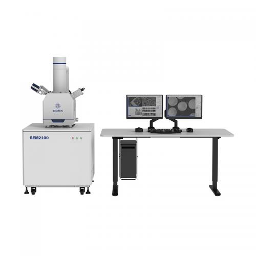
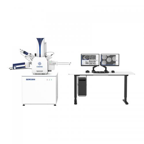
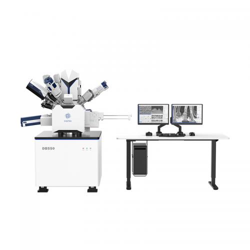
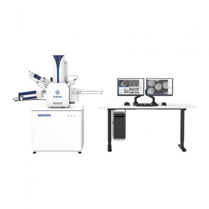
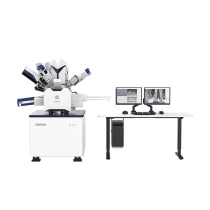
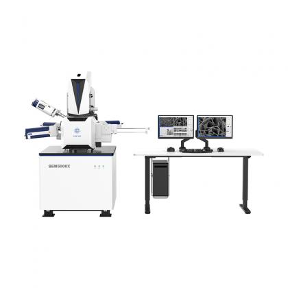
- Weltweiter Lieferant von Feldemissions-Rasterelektronenmikroskopen
- SEM EDX-, EDS-, EBSD-, BSE-, CL- und STEM-Detektoren
- Raster-NV-Magnetometer, Quantendiamant-Rasterkraftmikroskop, QDAFM-Anwendungen
- Hersteller von ciqtek Scan-NV-Zentrumsmikroskopen
- Weltweiter Lieferant für scannende NV-Magnetometrie
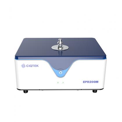
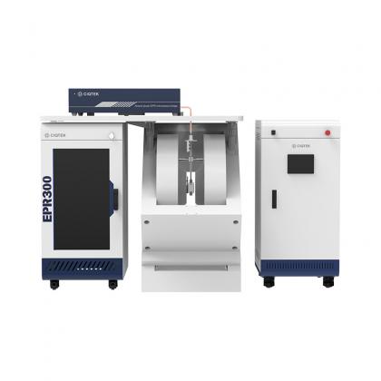
- Weltweiter Lieferant für X-Band-Puls-Elektronen-Paramagnetische-Resonanz-Spektroskopie
- Elektronenparamagnetische Resonanzspektroskopie Bester Preis
- X-Band-EPR-Spektroskopie mit Kryostat
- W-Band Elektronenparamagnetische Resonanzspektroskopie Bester Preis
- W-Band-Elektronenspinresonanzspektroskopie Bester Preis